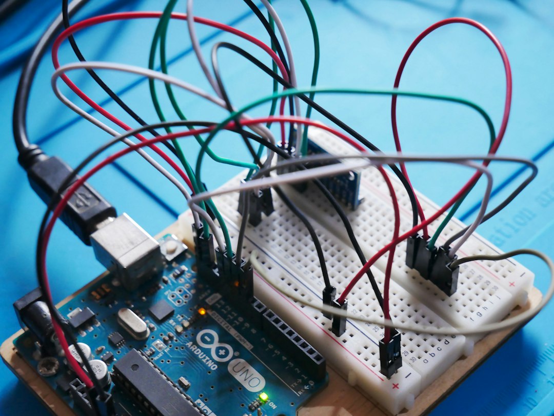
Why 3.3V Sensors Require Logic Level Converters With Arduino
Arduino boards like the Uno, Nano, and Mega operate at 5-volt logic levels, meaning their digital pins interpret a HIGH signal as approximately 5 volts. Meanwhile, an growing number of modern sensors—including the BME280, MPU6050, SSD1306 OLED displays, and many I2C peripherals—run natively at 3.3 volts. Plugging a 3.3V sensor directly into a 5V Arduino pin without translation can result in corrupted data reads, marginal signal timing violations, or outright hardware destruction over time. This is where a bi-directional logic level converter becomes essential infrastructure in any serious embedded project.
A bi-directional converter allows signals to flow both ways across the voltage boundary: from the 5V Arduino to the 3.3V sensor and back again. This dual-direction capability is critical for protocols like I2C and SPI, where the microcontroller must both send commands and receive responses across the same physical lines. Without bidirectional support, you would need separate unidirectional converters for each signal path—an expensive and space-consuming solution.
The most common applications involve I2C buses connecting multiple 3.3V sensors to a single Arduino, SPI-based display modules and memory chips, and even UART serial links where TTL level mismatches cause framing errors. Any project mixing 3.3V and 5V domains benefits from proper level conversion, and doing it correctly from the start prevents debugging nightmares later.
What Makes a Converter Truly Bi-Directional
Unidirectional converters translate signals in only one direction, which works for simple one-way data paths like sending a command from an Arduino to a sensor. Bi-directional converters, by contrast, use a feedback mechanism or dual-transistor topology that automatically detects signal direction and translates accordingly. The classic design uses N-channel MOSFETs arranged so that the higher voltage side pulls the gate through a pull-up resistor, creating a self-adjusting threshold that enables seamless translation in either direction. This architecture means a single chip handles both the SDA and SCL lines of an I2C bus without any external control signals determining traffic flow.
How Bi-Directional Logic Level Converters Work Internally
Understanding the internal operation of a logic level converter helps you diagnose failures, select the right component, and troubleshoot communication issues when they arise. The most widely referenced design is the single-MOSFET bi-directional translator found in chips like the TXS0108E and its predecessors. This circuit relies on three key elements: an N-channel MOSFET, pull-up resistors on both sides, and the inherent body diode of the MOSFET.
When the low-voltage side (3.3V) drives a line HIGH, the MOSFET turns on because its gate is pulled up toward the high-voltage side potential through a resistor. Once the channel conducts, the high-voltage side (5V) sees the line pulled down to near ground, establishing a valid LOW signal. When that same side goes HIGH, the voltage difference across the gate-source junction keeps the MOSFET off, allowing the pull-up resistor on the 5V side to drive the line to 5 volts independently. The same principle applies in reverse when the 5V side initiates a LOW state—the body diode and MOSFET action together ensure the 3.3V side interprets it correctly as a logic LOW.
For open-drain protocols like I2C, this arrangement works exceptionally well because both SDA and SCL are naturally bidirectional and require external pull-up resistors anyway. The converter essentially becomes an intelligent extension of those pull-ups, adapting their effective voltage to whichever domain the active driver belongs to. Push-pull outputs behave differently and may require additional consideration, which we will cover in the implementation section below.
Critical Parameters That Define Converter Performance
Several electrical specifications determine whether a given converter will work reliably in your application. First is the voltage range: your converter must support both the source voltage (5V for most Arduinos) and the destination voltage (3.3V for your sensor). Some advanced converters support wider ranges, including 1.8V to 5V, which provides flexibility when working with lower-voltage microcontrollers like STM32 or ESP32 devices.
Second is propagation delay—the time between a signal transition on one side and the corresponding transition appearing on the other. For slow protocols like I2C running at 100 kHz, delay is rarely an issue. At faster SPI clock rates above 1 MHz, however, cumulative delays across multiple channels can become problematic. The TXB0108, for instance, specifies a typical propagation delay of just 3 nanoseconds, making it suitable for high-speed applications.
Third is maximum data rate or frequency. I2C at standard mode (100 kHz) and fast mode (400 kHz) places minimal demands on any decent converter. Fast-mode plus (1 MHz) and high-speed I2C (3.4 MHz) require converters specifically rated for those speeds. SPI at 10 MHz or beyond demands the fastest available devices. Always check the datasheet rather than assuming compatibility based on package type alone.
Choosing the Right Converter IC for Your Project
The market offers several proven logic level converter integrated circuits, each with distinct trade-offs. Selecting the appropriate part depends on your protocol requirements, pin count needs, board space constraints, and budget.
The TXB0108 stands out as one of the most popular choices for general-purpose projects. This octal transformer features eight independent bi-directional channels, making it ideal for converting entire I2C or SPI buses along with spare GPIO lines. It operates from 1.2V to 5.5V on the high side and 1.65V to 5.5V on the low side, with a typical propagation delay of 3 ns and support for data rates up to 50 Mbps per channel. Its single-supply design means you only need to connect VCC to the 5V rail and let the device handle the rest internally.
The TXS0108E is another excellent option that builds upon the TXB0108 design with improved switching characteristics and lower quiescent current. It supports the same voltage ranges and channel count but introduces an enable pin that allows software control over when translation is active—a useful feature for power-sensitive battery projects where you want to disable unused converters.
For simpler applications requiring fewer channels, the TC4427 or CD74HC4050 offer straightforward solutions. The CD74HC4050 is particularly notable because it functions more as a unidirectional buffer with built-in level shifting rather than a true bidirectional translator. However, when paired with external MOSFET-based circuits or used selectively for one-way signal paths, it remains cost-effective and widely available.
Comparison of Popular Logic Level Converter Solutions
| Feature | TXB0108 | TXS0108E | CD74HC4050 | Module5 I2C |
|---|---|---|---|---|
| Bidirectional | Yes | Yes | No (unidirectional) | Yes |
| Channels | 8 | 8 | 6 buffers | 4 (2 per I2C) |
| Voltage Range | 1.2V–5.5V | 1.2V–5.5V | 2V–6V | 1.8V–5.5V |
| Max Data Rate | 50 Mbps | 50 Mbps | ~10 MHz | 400 kHz+ |
| Propagation Delay | ~3 ns | ~3 ns | ~10 ns | ~50 ns |
| Enable Pin | No | Yes | No | No |
| Typical Cost | $1.50–$3 | $2–$4 | $0.50–$1.50 | $2–$4 |
| Best Use Case | General purpose multi-sensor | Power-sensitive projects | Simple unidirectional needs | Quick prototyping I2C |
This comparison reveals that no single solution dominates every scenario. The TXB0108 and TXS0108E lead in raw performance and versatility, while the CD74HC4050 wins on price for unidirectional use cases. Pre-built modules sacrifice some speed for convenience and are perfectly adequate for most hobbyist and educational I2C sensor applications.
Implementing Bi-Directional Logic Level Converters for 3.3V Sensors
Setting up a bi-directional logic level converter follows a predictable pattern once you understand the underlying principles. The most common implementation involves connecting a 3.3V I2C sensor such as a BMP280, BME280, or MPU6050 to an Arduino Uno using a converter module placed between the two devices.
Begin by connecting the grounds of all three devices—Arduino, converter, and sensor—to a common ground point. This step is non-negotiable; without a shared reference potential, neither side can properly interpret logic states and communication will fail completely. Next, connect the Arduino's 5V supply to the HV (high voltage) power pin on the converter and the sensor's 3.3V supply to the LV (low voltage) power pin. Most converter modules include onboard regulators or simply pass through the connected voltages, so verify your specific module's pinout before powering up.
Route the I2C signal lines through the converter channels. Connect Arduino SDA to the converter's LA0 pin, converter LB0 to the sensor's SDA pin. Repeat for SCL using LA1 and LB1. If you are also translating GPIO lines for interrupt or reset signals, assign additional channel pairs accordingly. Power everything up and test with a basic I2C scanner sketch to confirm all addresses respond correctly before proceeding to full sensor integration.
Pull-Up Resistor Considerations for I2C Systems
I2C requires pull-up resistors on both SDA and SCL lines to ensure clean signal transitions. When using a bi-directional converter, you typically need pull-ups on both the high-voltage side and the low-voltage side. A standard starting value is 4.7k ohms on each side, though lower values like 2.2k ohms improve rise times at the cost of higher current consumption. For longer bus cables or higher I2C speeds, consider reducing resistance to 1k–2.2k ohms while verifying that your converter and sensor can source the resulting current.
Some sensors have internal pull-up resistors enabled by default, which can create conflicts when external pull-ups are also present. Check your sensor's datasheet and disable internal pull-ups if necessary to avoid parallel resistance networks that degrade signal quality. The TXB0108 itself does not require external pull-ups on its channels since the converter relies on whatever pull-ups exist on the connected buses, but you must provide them externally for the I2C protocol to function correctly.
Wiring SPI Devices Through Level Converters
SPI communication presents unique challenges because it typically uses four dedicated signal lines: MOSI, MISO, SCK, and CS. Unlike I2C, SPI is fully differential and each line has a designated direction, which means you still benefit from bi-directional converters especially for the MISO line traveling from sensor to Arduino. Connect Arduino MOSI through one converter channel to the sensor's MOSI pin, route MISO through a second channel in the opposite direction, and similarly handle SCK and CS lines as needed. Keep converter channel assignments consistent throughout your schematic to simplify debugging.
One important caveat with SPI is that some converters introduce slight propagation delays that can affect timing margins at high clock rates. If you are running SPI above 10 MHz, verify signal integrity with an oscilloscope or logic analyzer, and consider using converters with the lowest possible propagation delay specifications. For most practical Arduino projects running SPI at 1 MHz or below, any quality bi-directional converter will perform flawlessly.
Common Mistakes and How to Avoid Them
Even experienced builders make errors when integrating logic level converters, and these mistakes often manifest as intermittent failures that are surprisingly difficult to diagnose. Understanding the most frequent pitfalls saves hours of troubleshooting and prevents premature abandonment of otherwise sound designs.
The most common mistake is forgetting to connect grounds together. This single omission renders the entire conversion process meaningless because there is no reference voltage for either side to interpret logic states against. Always verify continuity between all ground points with a multimeter before powering on your circuit.
Another frequent error involves incorrect pull-up resistor placement. Placing pull-ups only on one side of the converter while expecting the other side to function correctly creates weak or missing signal transitions. Ensure pull-up resistors exist on both the HV and LV sides of every open-drain or open-collector bus line.
Exceeding the converter's specified voltage differential is a third critical mistake. While most modern converters handle the standard 3.3V-to-5V range comfortably, attempting to translate between 3.3V and 12V RS232-level signals or between 1.8V and 5V without confirming specification support can destroy the device instantly. Always verify the absolute maximum ratings in the datasheet before applying unfamiliar voltage combinations.
Capacitive loading on long wires or cable harnesses is an underrated issue that degrades signal quality at I2C speeds above 400 kHz. Each meter of cable adds capacitance that slows signal edges, and converters with finite output drive strength may struggle to compensate. Keep wire runs under 30 centimeters when possible, or reduce I2C speed to 100 kHz for long bus configurations.
Component Quality and Counterfeit Awareness
The hobbyist electronics market contains numerous counterfeit or substandard converter modules, particularly from unverified sellers on auction and marketplace platforms. Genuine Texas Instruments TXB0108 and TXS0108E chips carry clear marking, sharp silkscreen, and consistent packaging. Counterfeit versions may appear identical visually but exhibit degraded performance, excessive leakage current, or complete failure under load. Purchase from authorized distributors whenever possible, and verify authenticity by checking part numbers, date codes, and packaging quality upon receipt.
Real-World Projects Demonstrating Converter Applications
Bi-directional logic level converters appear in countless practical projects, and understanding real implementations helps cement theoretical knowledge. Consider a weather station building project combining a BME280 temperature-humidity-pressure sensor at 3.3V with an Arduino Uno at 5V. The BME280 communicates via I2C at 400 kHz, and a single TXB0108-based converter module handles both SDA and SCL lines alongside additional GPIO translations for a tactile reset button and LED status indicator—all within a compact breadboard layout costing under fifteen dollars in total components.
Another compelling example involves an IMU-based robotics platform using an MPU6050 gyroscope-accelerometer at 3.3V interfaced with an Arduino Mega. Here the converter not only handles the I2C bus but also translates PWM output lines driving motor controllers and digital input lines reading limit switches. The TXS0108E's enable pin allows the entire converter to be powered down during sleep modes, extending battery life significantly compared to always-on implementations.
Industrial applications extend further still. Factory automation systems frequently mix 3.3V PLC interface modules with traditional 5V relay driver circuits, and bi-directional converters provide the safe interface boundary that prevents ground loops and voltage transients from damaging sensitive control electronics. In these environments, robust converters with isolation ratings and ESD protection become standard components rather than optional accessories.
Building Your Own Custom Logic Level Converter Circuit
While purchasing pre-built modules is convenient, designing your own converter circuit deepens understanding and enables custom adaptations that off-the-shelf solutions cannot address. A minimal single-channel bi-directional converter requires only one N-channel MOSFET, two pull-up resistors, and a gate resistor—a component count that fits comfortably on a small strip of perfboard or even a veroboard layout.
Select a logic-level MOSFET such as the 2N7000 or BSS138, both of which turn on fully at 3.3V gate-drive voltages. Connect the MOSFET source to the low-voltage side, drain to the high-voltage side, and gate to the high-voltage rail through a 10k ohm pull-up resistor. Place a 10k ohm pull-up on the high-voltage side and another 10k ohm pull-up on the low-voltage side of the signal line. Add a small gate series resistor around 100 ohms to dampen ringing and reduce EMI emissions. This simple circuit translates I2C signals reliably up to several hundred kilohertz and serves as an excellent learning project before scaling to multi-channel implementations.
For multi-channel designs, replicate the single-channel block across however many channels you need, sharing the same gate bias network or using individual pull-ups per channel depending on your noise immunity requirements. Keep trace lengths short and symmetric to maintain signal integrity, and add decoupling capacitors near the power input to suppress transient spikes.